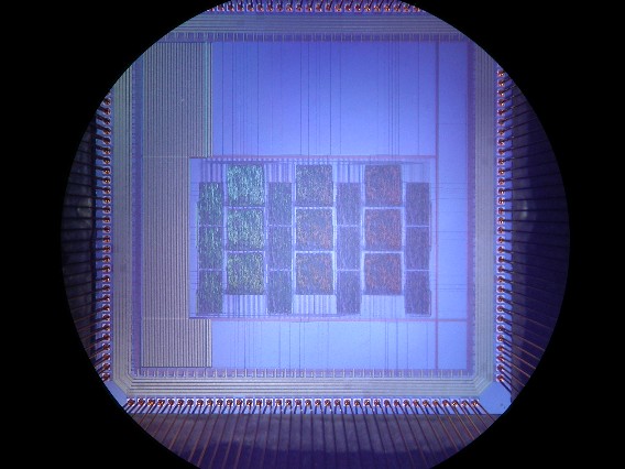
VDEC Rohm 0.35 micron, 4.9 mm x 4.9 mm
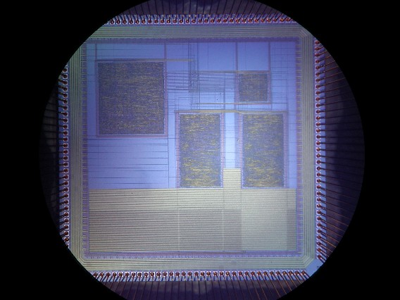
VDEC Rohm 0.35 micron, 4.9 mm x 4.9 mm
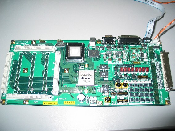
This is planned by Takeshi Ikenaga (and me) in our graduate school and made by MMS. We should thank to Kazutoshi Kobayashi of Kyoto University for his comments on the functions of the board.
Basically we have developped a VDEC chip test board at NAIST and this one is the revised board. The NAIST board was designed by Masaki Nakanishi with the support of Takashi Horiyama and me at 2000 - 2001.